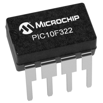
In this post we will explore how to implement an IR Emitter using a microcontroller, in this case a PIC10F322. I chose this microcontroller because:
- It’s cheap
- It’s tiny
- It has a PWM module, which will be very useful in creating the carrier signal
This solution is far from optimal because I frankly didn’t do much research beforehand. Since I only have eight buttons, a far easier way to solve this would be to pick a microcontroller with more inputs. Doing this would have reduced the total cost, overall power consumption, and code and circuit size and complexity. I might redo this project in the future, but for now, this is it.
This project is meant to be complimentary with an USB IR Receiver which is still a Work in Progress, aimed at controlling my computer from a distance while watching movies; for example to pause it or change the volume.
The full code for this project is available at https://www.github.com/aleixsanchis/PICRemote
The NEC Protocol
I decided to implement a standard protocol rather than a homemade one, as a learning exercise. Since I will also be the one implementing the receiver, it really wasn’t necessary, however this code can now be easily adapted to interface with a real appliance that uses the same protocol.
A multitude of protocols exist, but i chose the NEC one. It’s popular and well documented.
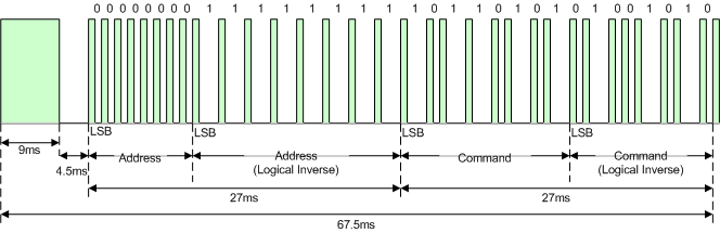
In the NEC protocol the messages are encoded as follows:
- Logical ‘0’: 562.5µs pulse burst followed by a 562.5µs space
- Logical ‘1’: 562.5µs pulse burst followed by a 1.6875ms space
A NEC transmission begins with a 9ms burst, followed by a pause of 4.5ms. This is immediately followed by the address of the intended receiver, LSB first. After the address, the inverted address is transmitted. For example, if we were transmitting for address 0b0000_0100, the inverted address would be 0b1111_1011. This is aimed at increasing the reliability of the protocol; if one value is not the exact inversion of the other, that means there was a transmission error and the message can be discarded.
After the address the actual command is sent, which will be interpreted by the receiver. And finally, followed by the command, the inverted bitwise value of the command will be sent, just like in the address. The frame is ended by sending a final 562.5µs pulse burst to signify the end of message transmission.
So, all in all, we got:
- a 9ms leading pulse burst (16 times the pulse burst length used for a logical data bit)
- a 4.5ms space
- the 8-bit address for the receiving device
- the 8-bit logical inverse of the address
- the 8-bit command
- the 8-bit logical inverse of the command
- a final 562.5us pause
Now, there’s a tiny detail left. While we are sending a burst, the signal appears to be a “block” or a continuous stream of data. However, that’s actually not true. The signal is modulated at a carrier frequency of 38Khz. This means that, actually, the signal is being switched on and off 38 thousand times per second. If we were to zoom in to a burst we would observe the following:
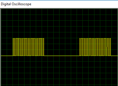
The reason of this modulation is to prevent other sources of IR to interfere in the transmission. For example, you can still use your remote in bright daylight, despite the sun being a source of infrared light much stronger than the tiny LED in the remote. This is because the receiver on your TV filters any signal that is not at that specific frequency (sometimes other frequencies are used, like 36 or 40 Khz).
The PWM module of the PIC10F322 will be very useful at implementing the carrier wave. It would still be possible without it, by bit-banging the output pin, but it makes it much easier.
Now that we’ve seen how the IR and NEC protocol works, let’s move on to our microcontroller.
The PIC10F322
This microcontroller contains:
- 0.896 KB Flash
- 64 B SRAM
- 16 MHz internal oscillator
- 4 GPIO (one of them is input only)
To program it we will use the MPLABX IDE with the XC8 compiler provided by Microchip. Both are gratis, but not free software and can be downloaded from Microchip’s website.
The circuit
Since I wanted my remote to have eight buttons, a Parallel-In Serial-Out (PISO) shift register was needed to have enough inputs. A PISO shift register is a device that allows us to increase the amount of inputs by storing a parallel set of data and then outputting them one by one on each clock. This way we can read the eight buttons with only 3 pins. In this project, I used a 74HC165 from Philips.
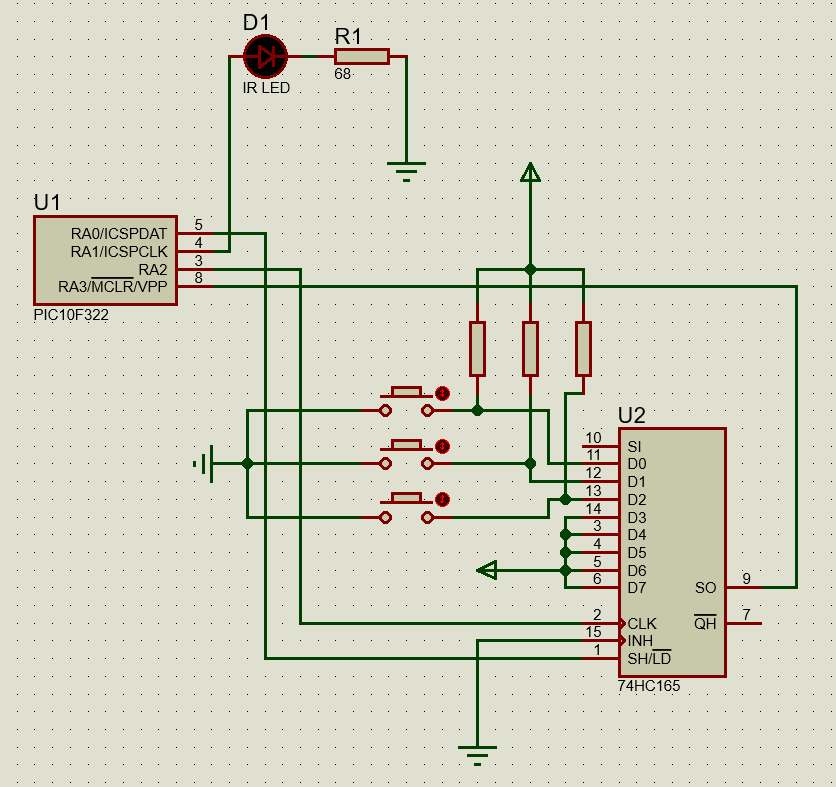
The pins are connected in the following way:
- RA0 (output) -> Shift Register SH/NLD. This pin controls when the inputs are loaded to the shift register.
- RA1 (output) -> IR LED. This pin is driven by the PWM module.
- RA2 (output) -> Shift Register CLK. On each rising edge of this signal, the register will shift a new value to its output
- RA3 (input) <- Shift Register Serial Output. This pin will read the state of the buttons.
Each button has its corresponding pull-up resistor, so a Low value will mean the button is pressed. As always, select a resistor for your LED according to its forward voltage and the desired current. A typical value is fV of around 1.5-1.7V and maximum current when pulsing is 80-100 mA. Because I don’t need a big range in my remote, 20 mA (the sink current recommended for the PIC GPIO) should be fine and thus I won’t need to drive the LED with a transistor.
The design of the circuit is not final yet, because some decisions are still not taken until I have to build it in a circuit board. I will probably run this circuit off a CR2032 or two AAA batteries in series, and still have not decided if a 3.3V regulator will be used or just connect it straight from the battery.
The Code
Device configuration
To configure the device I used the following parameters:
- Internal Oscillator at 8Mhz
- Watchdog Timer and Brown-out Reset Disabled
- Low Voltage Programming disabled (more on this now)
The PIC10F322 has 4 GPIO, but RA3, aside from being input-only, also serves as !MCLR. This means that, under “normal” conditions (with Low-Voltage Programming, LVP, enabled), the device would reset when this input is driven Low. To be able to use this pin as an input, LVP must be disabled. Then, to enter programming mode, RA3 needs a high voltage, in the order of 8-12V. For more information about LVP, and how to configure the device, consult the datasheet.
So, my configuration is as follows:
1
2
3
4
5
6
7
8
9
10
11
12
13
14
15
16
17
18
19
20
21
22
// CONFIG

#pragma config FOSC = INTOSC    // Oscillator Selection bits->INTOSC oscillator: CLKIN function disabled
#pragma config BOREN = OFF    // Brown-out Reset Enable->Brown-out Reset enabled
#pragma config WDTE = OFF    // Watchdog Timer Enable->WDT disabled
#pragma config PWRTE = OFF    // Power-up Timer Enable bit->PWRT disabled
#pragma config MCLRE = OFF    // MCLR Pin Function Select bit->MCLR pin function is digital input, MCLR internally tied to VDD
#pragma config CP = OFF    // Code Protection bit->Program memory code protection is disabled
#pragma config LVP = OFF    // Low-Voltage Programming Enable->High-voltage on MCLR/VPP must be used for programming
#pragma config WRT = OFF    // Flash Memory Self-Write Protection->Write protection off
// LFIOFR 31.25KHz_osc_not_ready; HFIOFS unstable; HFIOFR 16MHz_osc_not_ready; Oscillator at 8MHz;
OSCCON = 0x60;

// Set Port A to low
LATA = 0x00;

// We set up RA1 as an input; This pin drives the PWM. If set to input, the pin will be driven low
// when we want to drive the LED, we simply set it as an output
TRISA = 0x02;

// Set PORT A as digital GPIO
ANSELA = 0x00;
The main loop
In the following code block we see the main loop used in the firmware:
1
2
3
4
5
6
7
8
9
10
11
12
13
14
15
16
17
18
19
20
21
22
23
24
25
26
27
28
29
30
31
32
33
34
35
#define IR_OUTPUT PORTAbits.RA1
#define SHIFT_REG_SH_NLD PORTAbits.RA0
#define SHIFT_REG_CLK PORTAbits.RA2
#define SHIFT_REG_INPUT PORTAbits.RA3

void main(void) {
    // initialize the device
    SYSTEM_Initialize();

    while (1) {
        // LOAD INPUTS TO SHIFT REGISTER
        SHIFT_REG_SH_NLD = 0;
        // Make sure the inputs are loaded
        __delay_us(1);
        SHIFT_REG_CLK = 0;
        // ENABLE SHIFTING
        SHIFT_REG_SH_NLD = 1;
        // SHIFT EACH INPUT ONE BY ONE
        for (uint8_t i = 0; i < 8; i++) {
            // CHECK IF ANY INPUT IS PRESSED
            uint8_t input = SHIFT_REG_INPUT;

            // IF PRESSED (PULLED TO LOW) SEND TO IR EMITTER
            if (input == LOW) {
                ir_emit(i);
            }
            __delay_us(1);
            // RISE CLK
            SHIFT_REG_CLK = 1;
            // MAKE SURE THAT CLK STAYS LOW ENOUGH TIME
            __delay_us(1);
            SHIFT_REG_CLK = 0;
        }
    }
}
First, we initialize the device as needed (Oscillator, TRISA register, etc.).
Then, on line 12, we load new values into the shift register by bringing the SH_NLD pin of the register low. Then we iterate eight times, reading the register output. If any of the buttons are pressed (a low value), we send the value of the pin pressed. Since we are implementing the receiver, we can simply send the index of the button and interpret it on the receiver because we know the mapping. If you were interfacing with a real appliance you would need to find its address and the key codes used and send those instead. After that, we just shift the register rising and lowering the CLK pin of the register.
In the code I wrote delay statements to make sure the timing requirements of the register are met; according to the datasheet they shouldn’t be needed, but some caution never hurts.
Know that we’ve seen how the main program works, let’s see how we would implement the transmitter. First, we will set up the PWM module.
The PWM module
The desired parameters we want for our PWM signal is:
- 38 KHz frequency / 26.3µs period
- 50% Duty Cycle
The PIC10F322 Datasheet offers two formulas to determine the period (the inverse of the frequency) and the duty cycle ratio. However, the MPLABX IDE has a tool called Microchip Code Configurator. This tool allows us to easily configure aspects and peripherals of the device and avoid errors when doing the math. Don’t feel bad about using it, it’s a great time-saver.
First, we will have to configure the Timer 2, which is the source of the PWM module.
To get the desired Timer2 period, just introduce the value you want in the Timer Period field, in our case 26.3µs.
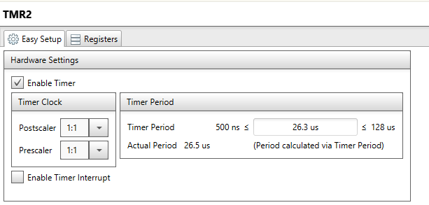
As we can see, our period won’t be exactly 26.3µs, but 26.5µs due to the available resolution. However, this slight difference won’t be much of a problem.
Then, we configure our PWM module using the Timer 2 as a source, and a duty cycle of 50%:
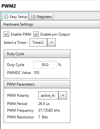
As we can see, the frequency of our PWM signal will be approximately 37.736 kHz instead of 38. This is a deviation of less than 1% so we should be fine.
And it’s just that simple. If it is your first time setting up Timers, it would probably be a good idea to configure them manually by reading the datasheet. However, once you know how it’s done, using the MCC saves you from a lot of time and helps you avoid bugs due to wrong calculations.
Driving the IR LED
So, now that we have configured the PWM to output our desired carrier signal, we just need to drive the LED and send data according to the NEC protocol. First, we will define two functions to start sending a PWM burst and to stop it.
1
2
3
4
5
6
7
8
9
10
11
12
static void send_pwm_burst() {
    TMR2 = 0x00;
    // PWM IS ENABLED BY SETTING RA1 back to an output
    TRISAbits.TRISA1 = 0;
    TMR2_StartTimer();
}

static void stop_pwm_burst() {
    TMR2_StopTimer();
    // BY SETTING RA1 to input, PWM is disabled
    TRISAbits.TRISA1 = 1;
}
As mentioned in the comments, a trick to easily start and stop the PWM pin is by simply setting the pin as an input. To do this, we simply write 0 (for output) or 1 (for input) in the corresponding bit of the TRISA register
Then, we just need to burst or stop the LED according to the NEC timings. For the header:
1
2
3
4
5
6
static void nec_send_header() {
    send_pwm_burst();
    __delay_us(9000);
    stop_pwm_burst();
    __delay_us(4500);
}
We simply burst for 9ms and then stop for 4.5ms. In these routines we used the delay macros provided by the XC8 compiler. The ideal approach would use Timer interrupts instead, so the device could do other tasks meanwhile instead of busy-waiting. However, in our device, there aren’t any other tasks to perform, so this approach is fine and simplifies the code.
To send a value, we start sending, from LSB first, each bit. If it’s a 1, a 562.5µs burst followed by 1687.5µs pause, or if it’s a 0, a 562.5µs burst followed by a 526.2µs pause. This function will work for both sending the NEC address and the command.
1
2
3
4
5
6
7
8
9
10
11
12
13
14
15
16
static void nec_send_value(uint8_t value) {
    for (uint8_t i = 0; i < 8; i++) {
        if (value & 0x1) {
            send_pwm_burst();
            __delay_us(562.5);
            stop_pwm_burst();
            __delay_us(1687.5);
        } else {
            send_pwm_burst();
            __delay_us(562.5);
            stop_pwm_burst();
            __delay_us(562.5);
        }
        value = value >> 1;
    }
}
Finally, we just need to complete a whole NEC frame: Header, address, bitwise inverse address, command and bitwise inverse command.
1
2
3
4
5
6
7
8
9
10
11
12
13
14
15
static void nec_send_frame(uint8_t address, uint8_t command) {
    // HEADER: 9 mS PULSE
    nec_send_header();
    // ADDRESS
    nec_send_value(address);
    // !ADDRESS
    nec_send_value(~address);
    // COMMAND
    nec_send_value(command);
    // !COMMAND
    nec_send_value(~command);
    // FINAL PAUSE
    stop_pwm_burst();
    __delay_us(562.5);
}
So the code to send a NEC frame is finished. Now we just need to implement the public function ir_emit()
1
2
3
4
5
6
7
8
9
void ir_emit(uint8_t data) {
    if (data == last_command_sent) {
        nec_send_frame(RECEIVER_ADDRESS, data);
        last_command_sent = data;
    } else {
        // TODO SEND REPEAT CODE
        nec_send_frame(RECEIVER_ADDRESS, data);
    }
}
The NEC protocol supports sending repeat codes to avoid sending the same command multiple times if the same key is repeatedly pressed. As of now, I have not implemented them, but would be a nice addition in line 7.
And we have finished our firmware. Remember that, if you have any doubt, you can consult the full source code at my repo. It’s not fully documented but I believe it’s quite clean.
I will update this post once I build the final circuit. Meanwhile, thanks for reading.